
Chipping Away at China’s Tech Advances
The U.S. may spark a new semiconductor revolution by harnessing the law and the federal budget. Nevertheless, that may be only a part of the equation.
“The federal government has got to be one of the largest customers for Hewlett Packard workstations, for instance,” said Geremy Freifeld, technology portfolio leader and laboratory fellow at Draper, a nonprofit research and development organization. Draper estimates that around one-quarter of semiconductor demand is state-driven.
Draper sees a path toward designing weapons-specific semiconductors at first and following an evolution into mass production.
“We’re going to start at the individual weapons-system level to fund the manufacturing, but for sustainability, I think that the amount of specific microelectronics the government will procure in the future will continue to grow. Right now they talk about defense-specific parts being less than 1% of microelectronic demand,” Freifeld said.
“We’re in an interesting time geopolitically with regards to a few key market forces and economic forces as it relates to the semiconductor market,” said Walt Gall, CEO of Coherent Logix.
After the chip shortages due to the pandemic and reports that Chinese technology could introduce strategic changes in the global balance of power, the United States moved to limit the access of the Asian country to the West’s latest scientific achievements.
“We want to maintain that leadership position, and we certainly don’t want to have that come into a risky situation, whether it’s compromising our economic prosperity or our national security interests,” Gall explained.
On October 7, 2022, the United States banned the export of the latest semiconductors, or chips, to the People’s Republic of China. The measure aimed at stopping the Asian country from utilizing technology “to produce advanced military systems including weapons of mass destruction; improve the speed and accuracy of its military decision making, planning, and logistics, as well as of its autonomous military systems; and commit human rights abuses,” according to a U.S. Department of Commerce release.
Beijing’s official reaction was limited at first. China’s official spokesperson fielded 11 questions in a regular Ministry of Foreign Affairs press conference. Only an Agence France-Presse (AFP) news agency journalist asked about the restrictions, and Foreign Ministry Spokesperson Mao Ning responded.
“By politicizing tech and trade issues and using them as a tool and weapon, the U.S. cannot hold back China’s development but will only hurt and isolate itself when its action backfires,” said Ning, a George Washington University alumna, a day after the U.S. release was published.
The inevitability of China’s technological rise has been the official theme since then. But all that glitters is not gold.
“The Global Times,” a state outlet, followed up the next day with a strongly worded editorial stating, “Only arrogant and ignorant people can truly believe that the U.S. can block the development of China’s semiconductor or other technology industries by these illegitimate means.” Meanwhile, the “People’s Daily,” the Chinese Communist Party’s official outlet, chose to wait.
On December 5, 2022, the party’s official periodical carried a short commentary on the restrictions titled “U.S. impedes fair competition by protecting own sci-tech hegemony.” It took the Communist Party 59 days to produce 99 words about a change Secretary of State Anthony Blinken called an “inflection point” in a speech delivered in October 2022.
Producing semiconductors requires engineering, raw materials and suppliers. This translates as an ecosystem. In the case of semiconductors for defense, a layer of security must be added.
“Most of the electronics that we do for national security, I would say, aren’t commercially viable because they’re either focused on extreme security, or radiation hardness and are precision instrumentation way beyond what a consumer product would require,” Freifeld said.
The CHIPS Act allocates funds to expanding knowledge, potentially allowing further development of the ecosystem for specific defense applications.
“We’re really hoping to leverage the CHIPS Act to produce state-of-the-art electronics,” Freifeld said.
The effects could ripple beyond the Department of Defense and reach all state and local governments in the country.
“I don’t want to say ‘low volume’ because what I think’s going to happen, honestly, and what I hope happens, is that, for example: if you take the government as an enterprise, as an enterprise customer, the federal government procures a lot of money in electronics,” Freifeld told SIGNAL Media in an interview.
If secure and efficient semiconductors could be present on all desks, research, development and manufacturing would find a sustainable business.
Chips mean an edge on Earth as it is in heaven.
“We want to make sure we are on the cutting edge of the sensor and semiconductor technologies that have to deal with the high-velocity data streams both in space as well as here on Earth,” Gall told SIGNAL Media in an interview.
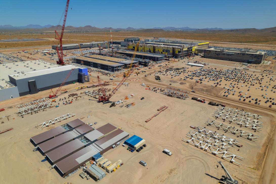
Behind sustainable production are two chip foundries building their semiconductor fabrication plants, or fabs, in Arizona: Intel and Taiwan’s TSMC. Both investments are under the auspices of the regulation. In some cases, there is an explicit intent to develop dual-use technologies.
“The government’s looking at setting up these prototyping capabilities that not only provide DoD with state-of-the-art capabilities and functionality but also contribute to the commercial space,” explained Roy Bishop, business development lead at Draper.
Still, to produce safe raw materials for electronics, the ecosystem must be wide. And machinery is not the only necessity for producing novel semiconductors. Chemicals, sometimes specifically synthesized for a particular chip, are another piece of a puzzle involving global trade with few suppliers.
Oftentimes unique sellers and coveted goods are virtually impossible to copy, even if a country successfully obtains, through any means, the blueprints and knowledge to reach the current technological pinnacle.
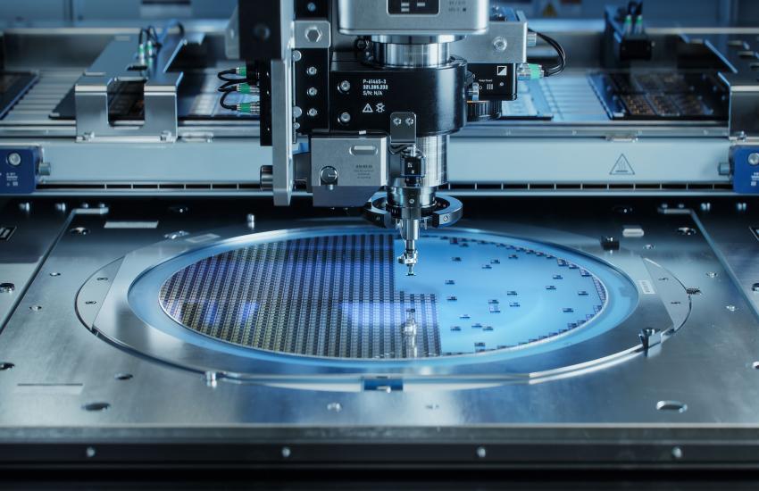
Chips are advancing toward smaller technologies than the denominated 3 nanometer (nm)—or three-millionths of a millimeter. These numbers speak about parameters that are not specifically sizes, according to Marc Swinnen, director of product marketing, Semiconductors, at ANSYS, an engineering firm that designs and tests chips.
And the passage into a 3 nm chip marks a major shift. It is not just about making a 7 nm but smaller.
Starting at 7 nm, extreme ultraviolet lithography, a new technology, must be employed. Only Dutch manufacturer ASML supplies these complex machines that harness laser beams at 50,000 pulses per second and tin plasma. Under these extreme circumstances, these rays are manipulated using precise mirrors, according to company documents.
ASML invested more than $6.4 billion in research over 17 years to have this unique position, according to the company. Therefore, today’s success is a result of planning in the early years of this century.
ASML declined to comment for this article.
The challenges of going under 7 nm are multiple. It is not only a question of obtaining the right machine from the Netherlands, from only one supplier that is closely observed by the U.S. government and has limitations as to which capabilities and knowledge it can share with China; the task’s complexity hits various roadblocks.
Copying the machine is virtually impossible, as ASML has thousands of suppliers that developed components to a level of precision that was part of that two-decade-long effort.
Still, to illustrate the size of the task, an expert offered just one of the problems he finds almost daily working on these technologies.
“At 3 nanometers, the wires are yet thinner, even thinner, even higher [electric] resistance, but it’s compounded by the fact that one of the primary performance metrics for a chip is power,” Swinnen told SIGNAL Media in an interview.
Design must consider not only the chip itself but also the current it receives from its device. Too much, and the semiconductor is degraded; too little, and it will not work.
Therefore, the technology around chips in a device is another angle that is often overlooked. And in those risks, specialists have suggested an opportunity.
Novel ways to array older generation chips could offer processing powers that could match current technology. This has been called 3D.
“Chip stacking, which is currently only employed in high-end operations like the production of high-bandwidth memory, has the potential to expand the number of transistors in a given volume—rather than an area,” said technology giant IBM in a report.
“The idea is that you’ll take two naked chips and put them right next to each other on another big chip called an interposer,” Swinnen explained. “You can take four or five chips and connect them together, make giant systems that still run as fast as if they were one chip.”
In this case, the options are endless, and China could skip limitations with this additive method instead of the nanometer road most headlines mention.
“3D is still reasonably in its infancy ... we’ll probably get there, but we’re nowhere near there yet,” Swinnen said.
China could well become a leader in this technology, but that will not happen soon.


Comments