DARPA Eyes Complex 3D Microelectronics

The Defense Advanced Research Projects Agency (DARPA) is helping to foster the next wave of microelectronics, the development and manufacturing of so-called three-dimensional heterogeneous integration (3DHI) chips, through a “robust” series of programs and efforts. To fortify U.S. microelectronics manufacturing for national security, the agency’s four-year-old Electronic Resurgence Initiative (ERI) is adding two new research areas—developing electronics for extreme environments and manufacturing complex 3D microsystems—as part of its so-called ERI 2.0 effort, reported Carl McCants, special assistant to the DARPA director, ERI, DARPA Microsystems Technology Office.
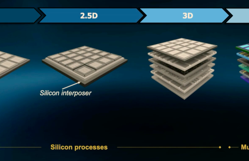
“[It is] a new era where we are leaving behind this simple device scaling and trying to push into where we are able to get higher performance, dictated by innovations in the third dimension,” McCants explained. “[With integrating heterogeneous components], it is where you’re stacking not one, not two, but three different layers. We went from things being separate to being together on a two-and-a-half-inch interposer, where we had active chips side by side, connected through a passive interposer layer. What we’re now focused on is 3D, where we are stacking things on top of each other, and what you will also see is the fact that we have changed the interconnection pitch [shrinking it 10-100 times]. We have changed the density. This shift from traditional monolithic manufacturing to the 3D changes the form factor.”
McCants spoke at The Ohio State University in October during DARPA Forward, which is a series of six conferences held between August and December at U.S. research and development universities to “energize regional and national innovation ecosystems to develop new breakthrough technologies for national security,” according to the agency.
ERI 2.0 will continue microelectronics research and development on how to: overcome security threats across the entire hardware life cycle; optimize designing and testing of complex circuits and prototypes; secure communications; realize heterogeneous 3D electronics; harness artificial intelligence hardware to make decisions at the edge faster; and increase information processing density and efficiency.
“DARPA is convinced, moving forward, that 3D manufacturing will further push the boundaries of performance, along with size, weight, power and cost,” McCants said.
The work also includes the creation of a national facility for 3DHI manufacturing through a public-private partnership with industry, academia and government under DARPA’s Next-Generation Microelectronics Manufacturing (NGMM). The effort will enable pre-competition collaboration with the partners in a unique facility.
“By establishing the first domestic, open-access facility for producing next-generation 3DHI prototypes, NGMM will launch a national accelerator in the form of a pilot-line manufacturing facility,” according to a DARPA statement. “Users from across the country can assemble and test their research and development designs without the need for costly investments. Instead, a wider variety of innovators can collaborate under a centralized, holistic approach to advancing, standardizing, and expediting domestic 3DHI prototyping.”
DARPA’s long-term goal with NGMM is to transition the developed capabilities to the National Advanced Packaging Manufacturing Program, which is associated with the National Semiconductor Technology Center, the agency said.
In October, the agency was starting to review the proposals it had received from its $20 million August Broad Agency Announcement for NGMM Phase 0 on how to plan the 3DHI manufacturing center, including specifications on how to construct “exemplar” 3DHI microsystems and all the necessary equipment, processes and facility needs for manufacturing the advanced microsystems. The agency expects to begin work under Phase 0 in February 2023 to plan the manufacturing center.
The more complex 3DHI boards will allow active chips that can be stacked on top of each other with bonding layers in between. The vertically stacked wafers can perform different functions from each other, e.g., a memory chip can be layered on a logic chip, he noted.
The chip materials will no longer be just silicon, the special assistant continued. And in future solicitations, DARPA will pursue contracts for the actual facility that will produce silicon-based and non-silicon-based 3DHI prototype systems.
“When we talk about 3DHI, we’re focused not just on silicon, but other materials: photonics, RF [radio frequency], MEMS [microelectromechanical systems], all of this stacked within a single package,” McCants explained. “We believe that now is the time for the community to push on technologies to manufacture complex 3D microsystems and put them into disruptive systems.”
Additionally, DARPA will delve into all aspects of 3DHI manufacturing systems research, including assembly and packing for multichip and multi-technologies; the tools needed for simulation, design and testing; security; interconnects; and thermal management and power delivery.

Indeed, the race is on for the United States to build its 3D microelectronics capabilities, as overseas, investments abound, McCants pointed out. Japan has invested significant funds, around $300 million, in a 3DHI public-private partnership as part of its Research Association for Advanced Systems. In addition, 20 companies from Japan’s semiconductor industry have joined TSMC’s 3D manufacturing research center. Singapore’s IME partnership is examining 3D bonding materials for vertical chip integration in a $210 million partnership at its Advanced Packaging Development Center, with chip manufacturer AMD involved.
In addition, the Taiwan ITRI’s Heterogeneous Integration Chip-let System Package Alliance, or Hi-CHIP program, is working to build an ecosystem for package design, testing and verification, and pilot production of 3DHI microelectronics.
For DARPA to succeed in its mission of growing domestic 3DHI capabilities, it is pursuing collaborative projects with six of the top 10 U.S. semiconductor sales leaders—Intel, Qualcomm, AMD/Xilinx, Samsung, NVIDIA and Micron—with all the top five U.S. defense contractors, with the top 10 research universities in America and with nontraditional partners.
“ERI must continue to strategically invest to seed new approaches and technologies to maintain our position in electronic systems,” McCants emphasized.
In regard to developing military electronics for extreme environments, DARPA will investigate three conditions in particular: high radiation, extreme temperatures and high power, which could include high voltage or high currents. “Each of these elements and conditions present their own unique challenges and opportunities,” the special assistant shared.
Lastly, McCants highlighted ERI’s early investigations and successes, including the creation of processor architectures that are 100 times faster than standard central processing units and graphical processing units, the development of programmable hardware architectures to increase processing efficiency, the integration of machine learning into tools for electronic design automation, the ability to process information while it remains encrypted and photonics integration of lasers on silicon wafers.
“It is possible to engage the academic, the commercial and the U.S. government microelectronics communities in relevant cutting-edge, dual-use research projects,” he noted. “It is possible to provide leap-ahead capabilities in computational efficiency, heterogeneous integration, hardware security, electronics design, artificial intelligence components and secure communications through these collaborations that benefit both the government and the private sector.


Comments