Detecting Microelectronic Defects
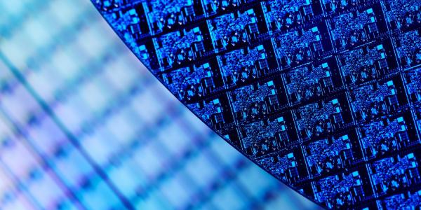
As semiconductor manufacturers aim to produce devices at the 5-nanometer node, the ability to find tiny defects created inadvertently during the fabrication process becomes harder. In addition, there is a growing need to verify that a chip was built as specified and doesn’t contain a malicious agent. Harnessing optical methods for semiconductor wafer inspection is one way to effectively look for anomalies, says Lynford Goddard, professor of Electrical and Computer Engineering (ECE) at the University of Illinois at Urbana-Champaign.
“In manufacturing semiconductor chips, there’s typically many steps in the fabrication process, and being able to see defects that are inadvertently introduced at different steps in the process is one of the grand challenges for the industry,” Goddard says. The professor, who earned a doctorate in physics and a minor in math from Stanford University, is head of Illinois’ Photonic Systems Laboratory within the Micro and Nanotechnology Lab.
While some deficiencies are benign, others are what Goddard refers to as killer defects that ruin the entire chip and can be extremely costly for a manufacturer. “These billion-dollar fabrication plants are processing wafers now that are the size of an extra-large pizza, 18 inches in diameter. A single nanoscale defect can, if it’s repeated across the wafer, ruin an entire wafer,” he states. “And these wafers cost millions of dollars each. One [sheet] gets cut up into thousands of different processing units with each of them retailing at $500 to $1,000 apiece, so you can imagine how important it is to avoid these killer defects.”
Moreover, finding defects in microelectronic wafers is not just about reducing the costs of consumer electronics and increasing the manufacturing yield, Goddard says. Sometimes, it is about security. Adversarial agents or malicious devices at a microelectronic level also have to be detected, especially as supply chain issues become more of a priority.
“It’s a question of how small of an object can be considered as a bad agent,” the professor estimates. “It’s possible for manufacturers to put in hidden components in circuits, and if they do it in a way that basically steals the security or creates a backdoor to loop in, being able to detect that and certify that the circuit contains exactly what it’s supposed to contain and nothing more, is critical.”
The problem is, as the nodes on a wafer become smaller and smaller, it becomes harder and harder to find a defect, Goddard notes. At that scale, being able to “see” a deficiency in terms of having enough of a signal-to-noise ratio for effective optical sensing is incredibly difficult. “When you look at the typical sensitivity or basically how strong a signal you get from the optical scattering of the defect, it scales very quickly with the size,” he explains. “Every time you shrink down the node, your signal gets weaker and weaker. If you cut the volume of the object in half, the intensity of what you measure tends to reduce by a factor of 64. So it’s a huge additional challenge every time, when you are battling with structures that are of a nominal size.”
In the mid-1980s, when transistors were made with 1 micron-sized features, nanoscale defects were not a problem, the professor says. But now with the small scale of modern transistors, at the technology node of 5 nanometers (in terms of half pitch), defects have a greater effect.
“With that structure, having one or two items out of place is enough to completely change the operating electrical characteristics of the device,” Goddard states. “So not only has being able to actually see these minor defects, in terms of having enough signal-to-noise ratio, become significantly more challenging, but also their impact on device performance has significantly increased.”
To differentiate between a defect, a malicious agent or a natural fluctuation in the manufacturing process, the researchers are harnessing optics or photon-based sensors. “Let’s say that you’re inspecting a 1-square centimeter piece of this wafer, inspecting a single die,” he says. “Typical lines of the patterns that make the devices are separated by 5 to 10 nanometers, and you want to be able to examine this dense pattern of design structures and look for any irregularities. [We look for] places where two lines are bridged together or … lines that are longer than they should be. We look for isolated defects that are going to influence the frequency response of the devices.”
Optical methods for semiconductor wafer defect inspection are more efficient, Goddard continues. Conventional methods for defect detection usually involve electron microscopy or atomic force microscopy. “The main disadvantage for those methods is that they’re slow,” he says. “They are serial scanning processes. And being able to inspect an 18-inch wafer would just take way too long.” The other drawback of the traditional methods is that they can be destructive to the wafer. “As you are probing with an atomic force microscope (AFM) or with a scanning electron microscope, the tools leave behind debris that damages the surface. And so it’s not practical for in-line inspection.”
Because optical imaging allows for inspection of a larger area—given a broader field of view—and offers higher throughput, optical techniques are promising, Goddard clarifies.
The researchers at the University of Illinois are also employing machine learning, applying algorithms to their optical methods that compare the measurements taken of a device versus a reference image. “We first run advanced image processing code to reduce measurement noise and then apply machine learning algorithms to find differences between figures or images,” he says. “Assuming that you are able to see differences, then that allows you to say, ‘Okay, there’s something that might not be quite right with this part of the circuit.’”
Almost a decade ago, Goddard, his collaborator, Gabriel Popescu, who is another ECE professor at Illinois, along with students, developed optical techniques for quantitative phase imaging of materials as part of a $2 million research instrument development grant from the National Science Foundation. Goddard explains that optical phase is a direct measure of the height of a surface versus position. “However, it is not something a camera can directly measure, so we designed and built a common-path interferometer at the output of a conventional microscope to encode the phase information into the intensity image that the camera measures,” he says. The team was able to obtain resolved height maps in high resolution.
“We developed a nondestructive optical method with the measurement accuracy of AFM but with a thousand times greater aerial throughput,” he notes. “[We] successfully observed nanoscale dynamics in situ, such as nanotubes while they roll up, water droplets as they evaporate, semiconductors while they etch and materials as they expand due to heat or chemical reactions.”
A few years later, the team applied the techniques to detecting semiconductor defects under a multiyear project funded by the Semiconductor Research Corp. The researchers looked at 22-nanometer and 9-nanometer node wafers, using chips provided by SEMATECH that contained a few intentional defects of different shapes and sizes.
“We knew that our methods would be sensitive to nanoscale variations in height, but we were pleasantly surprised that they were also sensitive to nanoscale variations in lateral dimensions even though these variations are too small to directly observe because of the diffraction limit,” Goddard shares. The researchers also developed image collection strategies as well as post-processsing algorithms that reduced different types of experimental noise.
Goddard’s lab now focuses more on theoretical work, including computational electromagnetic simulations, to design new types of optical imaging techniques to address the signal-to-noise ratio issue. “We’ve done a lot of work in terms of designing experimental configurations that will highlight certain defects,” he clarifies. Along with employing machine learning and developing better post-processing noise reduction algorithms for the optical imagery, the researchers are coming up with fundamental new ideas for experimental configurations that will emphasize a deficiency in a chip.
“It’s about increasing the signal-to-noise ratio in the experiments, increasing the signature of the signal or reducing the noise in post-processing, and then also increasing the ability to draw conclusions by applying machine learning to it,” the professor states. “You can model what the defects should look like, but your model is never perfect. It never exactly represents the experimental data, and so you can use both your model and your experimental data to train the machine learning algorithms so that when you get new experimental data, you can decide whether the data indicates the presence of a defect or not, even though you don’t have a visual representation of the defect.”
The researchers hope to have the opportunity to continue with their experiments by measuring possible defects using new chip samples, Goddard says. However, as the technology node of chips gets smaller and smaller, it’s much more difficult to get samples.
Here, the Illinois lab is looking for industry partners, or federal agency partners, such as the Department of Defense, for opportunities to perform research or to secure microchip samples, the professor notes.
“Fewer and fewer people can actually manufacture it,” he says. “A decade ago, chips at the 65-nanometer technology node were something that a hundred or so facilities throughout the world could make. A wafer at the 5-nanometer node was only realized last year by a team at IBM. This year, only two or three companies can manufacture a circuit that complex with that small of dimensions.”
The need from the semiconductor manufacturing industry to be able to validate circuits will only grow in the future, Goddard says.
“And from the research point of view at the university, our goal is to explore new technologies and explore new methods of doing things,” he shares. “How do you know that the circuits that you’ve built or the devices you built will function if you can’t measure it? So there’s an increased push from semiconductor manufacturers to be able to measure and verify circuits. And as components are now starting to get to these really small scales, how do you check and verify the circuits as the components shrink in size?”


Comments