Molecular Devices Burgeon
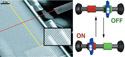 |
| A molecular switch is an important step toward building molecular computers. The Defense Advanced Research Projects Agency’s Applications of Molecular Electronics, or MoleApps, program sponsors research for two-state rotaxane molecules that act as switches. Designed in the University of California, Los Angeles, laboratory (r) the switches store information in an ultra-dense 160-kilobit memory made up of a 400 x 400 grid of nanowires (l). |
Promising advances in integrated circuit technologies such as nanowires, molecular electronics and fault tolerant architectures could help alleviate industry needs in designing and fabricating computer chips. New emerging technologies and approaches generally unknown to industry will be urgently required within six or seven years to help sustain continuing progress in dense integrated circuit production.
Applications of molecular electronics already are proving instrumental in developing nanotechnologies that provide a solid foundation for myriad capabilities and continuing development. Two technology thrusts include molecular computing and sensing—nanometer-scale logic, memory arrays, organic sensors and molecular mechanics. Impressive developments are emerging from the Defense Advanced Research Projects Agency’s (DARPA’s) Applications of Molecular Electronics, or MoleApps, program.
MoleApps technologies already are moving to industry and other military programs for a growing number of applications, according to Dr. Cynthia Daniell. She is the MoleApps program manager in the agency’s Defense Sciences Office. A senior research scientist at HRL, she received a bachelor’s degree in electrical engineering from the
Participating in the DARPA program is a CalTech research team, which created memory circuits the size of a human white blood cell with 160 kilobits of memory. This is believed to be the densest memory circuit ever fabricated, Daniell reports.
A Hewlett-Packard-led consortium with CalTech and the
This consortium is starting to fabricate chips on a 60-nanometer-pitch scale, which is expected to lead to fabrication of a 45-nanometer pitch. Progress in semiconductor integrated circuit technologies is gauged using the metric of pitch, or the most closely spaced wires within a dynamic random access memory (DRAM) circuit. Pitch wires for modern DRAMs are 140 nanometers, as an example. “When this program began several years ago, goals of a 30- or 40-nanometer pitch were very ambitious,” Daniell discloses. “Today, a California NanoSystems Institute [CNSI] switch can control individual molecules with voltage, allowing them to compress and expand, to open or close a valve.”
Two-state rotaxane molecules designed in the UCLA laboratory of J. Fraser Stoddart—who is the director of CNSI—act as switches to store information in an ultra-dense 160-kilobit memory made up of a 400 x 400 grid of nanowires. This demonstration is an important step toward molecular computers that are much smaller and more powerful than silicon-based computers. The consortium’s contribution includes superlattice nanowire pattern transfer for 30-nanometer crossbar memory and logic arrays.
The effect on industry is the introduction of molecular switches that could overcome the physical limitations of lithography-based integrated circuit feature sizes. The new technology also reduces power requirements, Daniell says.
With approximately $10 million in 2007 funding, DARPA’s MoleApps program is structured to demonstrate a programmable nanometer processor, or nanoprocessor, integrated on the molecular scale. The nanoprocessor would occupy a total area of 100 square microns. This minuscule device would operate at room temperature with logic and arithmetic processing capability comparable to the original Intel 4004 microprocessor. However, the molecular electronic computer would be 100,000 times smaller than the Intel processor and would be 100 times as dense as systems presently promised by industry, Daniell explains. Using methods of hierarchical nanofabrication and nanoassembly, the system will be much less costly to manufacture than those projected by the International Technology Roadmap for Semiconductors.
With teams from industry and academia participating, the DARPA MoleApps plan is to develop an ultra-dense molecular electronic computer processor with reliable fabrication of a prototype having local densities of at least 100 billion devices per square centimeter. Such a processor will have 50,000 nanodevices in a 100-square-micron area, all operating with a clock rate of at least 10 kilohertz or the equivalent. Power consumption would be no more than 10 watts per square centimeter.
MoleSensing, an ultra-dense molecular electronic sensing system, is another of the program’s goals. The thrust is to develop and demonstrate a nanosensor system that also is integrated on the molecular scale and occupies a total area of only 100 square microns. The sensor must be capable of detecting chemical or biological agents with sensitivity comparable to current state-of-the-art detectors. To achieve these objectives, 1,000 individual nanosensors would be placed in an ultra-dense array that occupies only 1 square micron. This nanosensor system must be capable of selectively identifying any of seven targeted chemical and/or biological agents. The system’s sensitivity would be 10 to 17 molar or better within 10 seconds, Daniell points out.
MoleApps’ main goal is to move forward in the nanoworld, where teams working with the agency are accomplishing much of the research, Daniell says. These teams include Hewlett-Packard, CalTech and UCLA working on crossbar arrays with molecules and nanometer field effects transistors; Harvard, Yale, the Georgia Institute of Technology, the University of Southern California and SRI working on semiconducting nanowires, sensing and three-dimensional electronics computing; Northwestern University with self-assembly and nanolithography; the University of Virginia, Rice, Yale, Purdue and SAIC working on hybrid molecule complementary metal oxide semiconductors; and Arizona State with unique capability for electron transport measurements.
“
The Dip Pen direct-write capability, positive printing and high-resolution capability offers 10-nanometer line width and 5-nanometer spatial resolution. Possible applications are DNA sensing with nanoprobes and on-wire lithography for nano/molecular electronics, plasmon waveguides and chemical and biological sensors. The impact on industry is opening several new areas of research in nanomedical and pharmaceutical technologies.
The MoleApps program is advancing the state of the art in ultraviolet-electron beam lithography beyond industry standards with ultra-dense logic and memory arrays of 15 nanometers. Defect tolerant architecture is another advantage, Daniell notes. “Because of low yields with nanoscale computing, creative methods had to be developed to use a computer when only 30 percent of the parts worked. Therefore, algorithms and hardware work-arounds were created. This situation, in turn, spawned many innovations so that systems would know and predict when and where a failure might occur—an adaptive, defect tolerant architecture,” she adds.
It has taken several years for the high-risk and high-payoff MoleApps program to bridge the gap between breakthrough discoveries and applications. However, on the current path, numerous military and commercial developments are harnessing MoleApps technology and employing it with entirely new genres of product lines and systems.
Web Resources
DARPA MoleApps: www.darpa.mil/dso/thrust/matdev/moleapps.htm
CNSI at UCLA: www.cnsi.ucla.edu
Agency Boosts Direct-Write Lithography A program underway at the Defense Advanced Research Projects Agency (DARPA) aims to develop maskless, direct-write nanolithography for defense applications. If successful, it will reduce costs greatly and widely expand the use of microelectronics. This program is based on writing circuits versus printing them to provide a cost-effective manufacturing technology for highly customized application-specific integrated circuits, or ASICs. DARPA has a co-funded joint development agreement with an integrated circuit tool manufacturer to produce a direct-write, maskless lithography tool. When installed in the trusted foundry and in commercial foundries, this tool would enable state-of-the-art microelectronic circuits to be used in new military systems and to upgrade legacy systems cost-effectively. Today, it is very expensive to develop masks needed for the typical process of printing ASICs. These costs pose a particular problem for the U.S. Defense Department. High-volume production can amortize the high costs of masks across many chips; however, the department generally needs only the low volumes that are characteristic of ASICs. The current cost of a mask can make defense-specific chips expensive and threatens to limit the use of leading-edge microelectronics by the department. |


Comments