Novel Electronic Devices Emerge
 |
| Multiple military applications of the technology are driving development of Wide Bandgap Semiconductor for Radio Frequency (WBGS-RF) materials. Industry teams are developing monolithic microwave integrated circuits, MMICS, and devices for applications that include systems such as the Army’s Theater High-Altitude Area Defense (THAAD) antimissile system radar. The technology enables transmitting with higher power and reduced cooling and receiving in higher dynamic range. |
An engine of innovation, the Defense Research Projects Agency’s Microsystems Technology Office relentlessly drives down the size, weight and power requirements of ever-higher-performance electronic components. Its development of semiconductor materials for innovative electronic devices places this organization on the cusp of major breakthroughs with next-generation communication, radar, electronic warfare, imaging and sensor systems.
Programs with far-reaching implications include the Wide Bandgap Semiconductor for Radio Frequency (RF) applications (WBGS-RF) and Technology for Frequency Agile Digitally Synthesized Transmitters (TFAST). Both programs involve III-V semiconductor materials. WBGS-RF is showing striking improvements in power-added efficiency, gain, bandwidth, power density and reliability. Meanwhile, TFAST is demonstrating direct digital frequency synthesizers that advance the state of the art by a factor of three in clock frequency, with high spur free dynamic range over a large bandwidth.
Improving the features of WBGS-RF devices will provide a variety of military roles. Applications include X-band transmit/receive modules used in radar assemblies, Q-band high-power amplifiers for satellite communications and wideband high-power amplifiers for electronic warfare, explains Mark Rosker, WBGS-RF program manager. The technology is aimed at revolutionary methods of exploiting the properties of a class of materials, wideband gap semiconductors, for enhancing the capabilities of microwave and millimeter-wave monolithic integrated circuits (MMICs).
Innovative processes for fabricating several types of wide bandgap semiconductor materials are critical elements of the program. These materials include silicon carbide (SiC), gallium nitride (GaN) and nitride-based alloys such as indium aluminum gallium nitride (InAlGaN). “The goal is to develop the next generation of power amplifiers that are extremely important to a range of communications and sensor systems,” Rosker explains. He received a bachelor of science degree in physics from the California Institute of Technology and master’s and doctoral degrees in applied engineering physics from
The amount of power available determines range and sensor capability. “Better power amplifiers provide a big advantage in tactical situations,” Rosker notes. “However,” he quickly adds, “the importance of this technology is not only about power. What you get is much more than greater power. You also get more bandwidth and higher power-added efficiency for more effective operations.”
Power-added efficiency is the more critical technical advance, especially in terms of radar applications. “Every watt you don’t send out the front end of the radar antenna means having to control heat, and that becomes a critical operational factor. In some applications or situations, changing the power-added efficiency by even 5 or 10 percent has an enormous impact on the sensor system,” Rosker claims.
WBGS materials have about the same lattice constant, so that one material can be grown on top of another—such as GaN on a SiC substrate to fabricate a power amplifier. Power density of these devices, which is a common metric—number of watts per millimeter of the length of the transistor gate—is typically 10 times higher than with today’s gallium arsenide. “That is an enormous number; you rarely see electronics 10 times better than ones possibly being replaced,” Rosker offers. “There is a compelling reason to build WBGS-RF power amplifier devices—some short devices in the program have demonstrated 40 watts per millimeter, or 40 times higher than today. But key for the program is a high-performance power amplifier MMIC that is reliable and that will not degrade.”
The program is a comprehensive effort to establish capabilities to design, fabricate and demonstrate wide bandgap devices with high performance and reliability at an affordable cost. A specific program objective is to understand degradation mechanisms of WBGS devices, which would lead to robust, highly reliable devices and MMICs, according to Rosker. DARPA must be certain that GaN MMICs will not degrade within a few minutes, which sometimes can occur with this material. “To have a useful device, we need thousands, hundreds of thousands or millions, 106 hours that users typically want. The central challenge in the program is to understand the physics of why these materials might degrade when used at realistic stressing levels of performance,” he declares
In addition to 106 hours of reliability, Rosker points out, technical challenges also involve a high operating frequency of 40 gigahertz, a high bandwidth of 1 decade, RF yields of 50 percent and thermal management of approximately 1 kilowatt per square centimeter.
By DARPA standards, WBGS-RF is a long program. The first phase of the program lasted two years and was related to materials research involving some 12 universities. The second phase is underway now, and it is an 18-month three-track effort involving three-dimensional devices. Each program track has a slightly different goal. However, all of the tracks involve building power amplifiers out of GaN on SiC.
Track 1, which focuses on efficiency, involves X-band transmit/receive modules—transmitters with higher power and reduced cooling and receivers with higher dynamic range and lower system RF. Raytheon, Andover, Massachusetts, is teamed with Cree, Durham, North Carolina, to provide a power-added efficiency of 60 percent at 8-12 gigahertz, which is much higher than with widely used GA material, Rosker reveals. In general, WBGS-RF module characteristics are expected to be equivalent to or better than those of current transmit/receive modules capable of delivering 10 watts continuous wave output power over the same frequency range. The Track 1 team is working toward a power amplifier MMIC that meets performance requirements. Possible applications include the Theater High-Altitude Area Defense (THAAD) system.
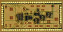 |
| A team from BAE, Vitesse and University of Illinois, Urbana-Champaign successfully developed a 5,000-transistor, 30-gigahertz direct digital synthesizer with a 15-gigahertz output and 30 percent yield at full RF specifications. The technology application is aimed at ultra small but powerful electronic warfare systems for use on micro air vehicles. |
The third track—wideband—involves building a power amplifier with a power-added efficiency of 20 percent operating in a frequency range of 2 to 20 gigahertz. Operational bandwidth would be 1 decade, with a pout of 100 watts and a module gain of 30 decibels, Rosker asserts. The prime contractor is TriQuint Semiconductor,
The 24-month third phase of the WBGS-RF program is slated to begin in March 2008 with electronic integration and circuit technologies. “We have made a lot of progress and are significantly far along in the program with all of the teams doing excellent work to this point. One of the issues is to find ways to conduct accelerated life cycle testing. How do you measure 106 hours without having to wait that long? We must use acceleration and some extrapolation.
“We already are in the thousands of hours in Phase 2. The program could change the whole III-V industry as GaN becomes available for this new technology, which is clearly better than we have today,” Rosker states. “And, the commercial implications are huge.”
Steve Pappert manages the TFAST program, which started in 2003 and is in the early stages of Phase 3. He earned a Ph.D. in electrical engineering from the
The DARPA development focused on a wide array of applications for high performance mixed signal, combined analog and digital circuits. The goal is to develop high frequency digital synthesizers and related circuits with high dynamic range, low phase noise, low power consumption and wide bandwidth, he explains. The preferred transistor technology for such circuits needs to have extremely high speed, high unity cutoff frequency (Ft) and high maximum frequency oscillation (Fmax) and high breakdown.
“The goal is to develop InP transistor technology for ultrahigh speed. The program addresses all aspects of development from materials, device design, device processing, circuit analysis, interconnects and integration in three phases,” Pappert reports. “Phase 1 involved technology pushing the effort to establish a viable super-scaled InP HBT that is more planar, lower power and capable of integration levels of 20,000 transistors and above. The second phase is an extension of the first to demonstrate complex mixed signal circuits.”
InP is a binary semiconductor composed of indium and phosphorus. It is used for high-power and high-frequency electronics because of its superior electron velocity compared to the more common semiconductors silicon and gallium arsenide. “HBTs generally lattice matched to InP offer the best combination of carrier transport and electrical breakdown but have been restricted by a lack of truly scalable device topology and processing approach,” Pappert points out.
“When the program started, we were at the stage with MMIC-types of technology using small numbers of transistors. The principal goal was to take InP technology and scale it in frequency and speed and simultaneously in complexity—to go from tens of transistors to thousands. This amounted to developing a lot of manufacturing processes to put InP on pace with silicon germanium (SiGe) and silicon complementary metal oxide semiconductor (CMOS) technologies,” Pappert illustrates.
InP transistor speed provides applications to communications, radar and electronic warfare by addressing front-end circuitry—very-high-speed amplifier technology, mixed signal circuits and analog-to-digital conversion. The focus of TFAST is on the direct digital synthesizer, which essentially is a digital-to-analog converter, or DAC. The device is configured in a way to synthesize signals digitally up to 20 gigahertz for electronic warfare attack. Digitally synthesizing wideband signals also can counter jamming. The development of direct digital frequency synthesizers can advance the state of the art in clock frequency over a large bandwidth by a factor of three.
TFAST provides a military effect by making available an unmanned digital electronic attack capability with stand-in, agile, coherent and low-power jamming from small platforms. “Communications are another application of TFAST advances,” Pappert discloses. “Encoding wideband, high spectrally efficient, complex, amplitude phase waveforms enables transmitting much more information, or capacity, within a given bandwidth. The program is demonstrating that the DDS, or encoder, will enable very high-capacity RF communications technology.”
Pappert remarks that InP technology properties enable exceeding high-speed, mixed signal performance in terms of Ft and Fmax, which have been dominated by Si and SiGe. The fundamental transistor dictates the types of circuits, circuit speed and ultimately performance. InP provides material with very high saturation velocities that far exceed Si and SiGe in current approaches. InP’s much higher breakdown voltage also provides linearity and high resolution for a DAC and a DDS.
Until recently the issue has been in scaling technology. For DAC or DDS devices, 5,000 to 10,000 transistors are required to build a circuit. No manufacturing process yields were available to produce large-scale integration using existing methods. DARPA embarked on the TFAST program to make a manufacturable InP technology available.
Contractor teams include Teledyne Scientific, Thousand Oaks, California, with the University of California, Santa Barbara; HRL Laboratories, Malibu, California, with the University of California, San Diego; Northrop Grumman Space Technology, Los Angeles; and BAE Systems, Nashua, New Hampshire, with Vitesse Semiconductor, Camarillo, California, and the University of Illinois, Urbana-Champaign.
The BAE/Vitesse team met all of the Phase 2 requirements and moved on to Phase 3, with other teams possibly close behind, Pappert acknowledges. “They have shown a 5,000 transistor DDS with essentially 15 gigahertz signal output, a dynamic range of greater than 40 decibels, 6 bits over the full 30 gigahertz clocking speed, and well over the 30 percent AC yield.” The BAE/Vitesse goal is to use the technology in an electronic attack system with capabilities well beyond standard non-solid-state standoff jamming pods now being flown.
The BAE/Vitesse approach would allow replacing the whole front-end chain of mixers and up converters with a simple synthesizer. This technology can synthesize any signal up to 15 gigahertz and any waveform that has up to 15 gigahertz of bandwidth, Pappert emphasizes. The technology offers strong electronic warfare appeal, and the BAE/Vitesse approach is to put a jammer on the DARPA Wasp micro air vehicle—with its weight of less than 200 grams and a 13-inch wingspan—or the U.S. Marine Corps Dragon Eye.
Three of the contractor teams are pressing to move from the $20 million second phase of the program and enter an up to $15 million third phase of TFAST, Pappert confirms. The other teams, however, continue in Phase 2. During the second phase, Ft/Fmax of 400/450 gigahertz was achieved, along with 5,000 transistors and at full RF specifications. The third phase involves mixed signal circuits with 20,000 transistors, 50-percent yield at full RF specifications, system demonstration and insertion.
Because of the significant size and weight reduction, TFAST devices can be used on small unmanned aerial vehicles. Scaling to smaller sizes and higher complexities reduces the power per function. Full DDS circuitry is being developed with 50-watt total wall plug power consumption. The program’s vision is to provide super-scaled ultra-fast InP HBTs in complex mixed signal circuits, which will enable three times higher circuit speed, 10 times higher integration and 10 times lower power.
TFAST’s goals are being met. Key accomplishments to date include the world’s fastest transistor at better than 50 gigahertz in Ft/Fmax, and the world’s fastest DDS with an output frequency from 0 to 15 gigahertz with yield, according to Pappert. The program is on track to develop terahertz clock speed transistors.
Web Resources
DARPA WBGS-RF program: www.darpa.mil/mto/programs/wbgsrf/index.html
DARPA TFAST program: www.darpa.mil/mto/programs/tfast/index.html


Comments