Nanomaterial Fabrication Moving to Desktop
A new printing technology could move the production of nano-sized electronic components from multibillion-dollar facilities into the hands of users, including military users in the field. The device, which is about the size of a desktop printer, will allow rapid prototyping of nanomaterials, contribute to stem cell and other medical research, offer a range of commercial uses and save potentially billions of dollars. Furthermore, because the product builds upon already widely available technology, it could be fielded within two years, researchers say.
Currently, nanomaterials are fabricated in multibillion-dollar facilities known as foundries; but with the new technology, those materials can be produced at low cost at the point of use. “What we created is a device akin to the desktop printer for nanofabrication. We think it is going to effectively take these very expensive foundries and make that type of capability accessible to anybody who wants to rapidly prototype or do small batch production, whether you’re talking about the electronics industry, the life sciences or other industries,” says Chad Mirkin, Northwestern University’s George B. Rathmann professor of chemistry, Weinberg College of Arts and Sciences. Mirkin also is a professor of medicine, chemical and biological engineering, biomedical engineering and materials science and engineering, as well as the director of Northwestern’s International Institute for Nanotechnology.
Normally, nanofabrication also requires the development of a mask to help define the lithographic pattern. A photo mask, for example, will form a pattern when polymer-coated materials such as silicon are exposed to light. These masks sometimes can cost millions of dollars. “This tool is going to be used to make these things called masks that are required to make custom electronics. It has the prospect of significantly decreasing the price and lowering the hurdle to changing things and making things on the fly,” Mirkin asserts.
The research, largely funded by the Defense Advanced Research Projects Agency (DARPA), the Air Force Office of Scientific Research and the National Science Foundation, one day may provide the military unprecedented flexibility. “We showed we can make all sorts of electronic devices—resistors, actuators and acoustic wave devices,” Mirkin reveals. “The military has all kinds of needs for electronics and optics devices. Sometimes, they need them fast. They need them on the fly and they need them sometimes generated in the field. This is a tool that will allow that.”
The research focuses on a tip-based nanofabrication process referred to as dip pen nanolithography (DPN). Mirkin was instrumental in inventing DPN in 1999, and he and his team continue to expand its capabilities. DPN uses an atomic force microscope, which can produce an image on virtually any type of surface, including polymers, ceramics, composites, glass and biological samples. The atomic force microscope is used as a cantilever, the tip of which acts as a pen. “We can coat these cantilevers with molecules that can transfer from the tip to a surface like ink transfers from a pen to paper,” Mirkin explains. Researchers are able to design the molecules to react chemically to the imaging surface to generate a structure one molecule high. The structures are made in a particular pattern—a circuit, diagram or spots for some cases involving medical research on DNA or proteins. “That was one of the first examples of nanomanufacturing. You could begin to make tiny nanostructures out of just about anything that could transfer from the tips to a surface,” Mirkin states.
Over the next 10 years, Mirkin and others developed tools to use cantilevers in parallel. Arrays of cantilevers can simultaneously deposit molecules onto a surface. “We made as many as 65,000 in one square centimeter—little tiny ends all working in parallel. All of those were effective either writing or not writing at the same time. Whatever you did with pen number one, you did with the other 64,999 pens of the array,” Mirkin adds. “Much of that technology was actually commercialized and sold all over the world for doing research-grade nanolithography. The technique is now used in more than 22 countries and hundreds of different laboratories both in academia and in industry.” That wide availability of much of the technologies means the latest innovations could be fielded in as little as two years, Mirkin adds.
Until recently, however, the technology was limited. “The problem is that as you begin to scale using that particular approach, adding more cantilevers and more capabilities, the arrays become more complicated and frankly, prohibitively expensive,” Mirkin reveals.
Next, the researchers began looking for a simpler, more scalable solution. They realized that the cantilever essentially acts as a spring, and they created a mold for producing a series of tiny pyramid shapes out of a spongy, polymer material to act as the tip. By filling the mold and placing a glass slide over it, they essentially create a rubber stamp of tiny pyramids. “It turns out we can make a lot of pyramids really cheaply. I can make an array where I have 11 million pyramids scanning a 3-inch-diameter circular mold. Each of those tips then can become a replacement for a cantilever. And all of that costs less than a dollar to make,” Mirkin reports. Researchers can now coat the pyramids with molecules, put that into an atomic force microscope and perform nano-scale dot-matrix printing. “It’s a radical change in thinking where we’re moving the spring defined by the cantilever to a spring in a tip made out of an elastic polymer material. The sponginess of the tip acts as the spring,” Mirkin says.
Still, he and his team had one hurdle to overcome. Regardless how many tips they used, all of them worked simultaneously. If one was in operation, all were. “All you have is a great duplication tool. Whatever you do at pen number one, you do at the other 10,999,999 pens in an 11- million-pen array,” he states.
The team next placed tiny heaters behind each tip, between the glass and the polymer stamp. “If you heat locally one of those pyramids, it pushes it in contact with the underlying substrate. So now, I can independently address each of these pens and simultaneously make different nanostructures on a surface in parallel,” he elaborates.
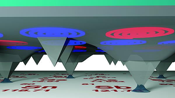
For one scientific paper, the team simultaneously wrote all of the atomic numbers for all of the elements on the periodic table using a different pen in a 16-pen array. “That shows that we have high resolution, the ability to print with molecules, the ability to print over large areas and the ability to make any independent structure,” he says.
The next innovation involved coating the polymer with a thin layer of gold and making a hole in each pyramidal tip to allow light to shine through it, a form of photo lithography in which chemicals are exposed to light to create an image or pattern. Normally, a photo mask, an opaque plate with holes or transparencies, is used with a photoresist, a polymer sensitive to light exposure, to form the pattern. “We can use a process known as reactive ion etching to shave a tiny little aperture at each of the tips of the array. If you shine light on the back of the array, you create 11 million beams of light,” Mirkin points out. “We don’t need a mask. We can take the array, shine light through the back of it, squeeze the light through these tiny little apertures and develop the photoresists on the substrate with nanoscale control.”
This innovation offers other advantages as well. “We can move the array with the precision of an atomic force microscope, so we can control how it moves on the nano scale,” Mirkin says.
But the “really cool thing,” Mirkin contends, is the use of a micromirror device, which is used widely for televisions. “We use this micromirror device to break up a [light-emitting diode] beam into many thousands of beams of light, and then we channel that light down each of the pyramids independently. We can turn them on or off selectively.”
The device can work with virtually any nanomaterial. “We can make anything. We can print anything that can be developed with light and anything that can be made to diffuse from a tip to a surface. And that’s a lot of things,” Mirkin emphasizes. And the potential uses are virtually unlimited. “There are uses across the board, across every industry,” he declares.
Mirkin says medical research will be a primary use for the device. “This is a tool that’s going to be used in many different fields, so it is going to enable rapid advances not just in electronics and photonics but also in the life sciences,” he says. For example, the device can be used to print and generate patterns of DNA and proteins, and will be useful in stem cell research. One major field of study focused on stem cell differentiation examines how different chemicals affect stem cells and drive the cells to grow into muscle, bone or other types of organic matter. Mirkin and his colleagues are building massive libraries of the chemical cues that spur stem cells in one direction or another.
Mirkin compares the technology to the desktop printer, which revolutionized the printing process. “This allows you to do nano- and microfabrication at the point of use and to create structures with the quality that we expect from a fabrication, but in a way that we don’t have to produce an expensive mask or get time on a multibillion-dollar piece of instrumentation or multiple pieces of instrumentation,” he says.
Still, he allows that comparisons to 3-D printing also are fair. “It is a type of 3-D printing, but it’s more than that. It’s a point-of-use nanofabrication tool. I like to think of it as a desktop fabrication instrument. There is a 3-D printing component to it on the nano scale because we can build layered structures as well, and we can build structures from the bottom up. But most of the things we’re building right now are 2-D, not 3-D,” he clarifies.
The DARPA project ends this year, but researchers may just be beginning to realize the technology’s potential. Mirkin says that in the coming years he and his team will continue to make the device smaller, faster and more flexible. “It will be part of many other projects that will be run by agencies that span the National Science Foundation, the National Institutes of Health, Department of Energy and the Defense Department,” he concludes.


Comments