Nanowire-Based Memory Technology Records Movement, Pressure
Physical movement stored as memory in a microchip could lead to advances in touch screens, robot control devices and medical implants. Researchers are arraying nanowires on a microchip to form a write-read memory cell as part of ongoing work that could convert motions, such as a hand in a glove or pressing a display, into memory. Moving or putting pressure on the nanowires creates an electrical current that can be read and recorded as memory. Arrays of such cells offer the potential for a variety of user interface applications and for new ways to convert mechanical or biological actions into electronic data.
Developed by researchers at the Georgia Institute of Technology (Georgia Tech), the piezoelectrically modulated resistive memory (PRM) system relies on the piezoelectric effect, where some materials, in this case zinc oxide nanowires, will generate electrical current when they are put under pressure or moved, which causes them to temporarily bend or deform. Piezoelectric materials also create mechanical strain (movement) when they are exposed to an electric current. PRM technology allows the creation of a new type of transistor that is switched on or off through movement or mechanical activity, explains Zhong Lin Wang, regents professor in Georgia Tech’s School of Material Science and Engineering in Atlanta.
Current memory systems, such as flash memory, are mainly if not entirely electronic, Wang says. But PRM technology allows the direct writing of electrical or optical memory through physical means. “Once you introduce the piezoelectric effect into the memory, you talk about the memory of strain and stress,” Wang notes.
By using electromechanical action to create memory, the system can mimic some biological systems. There are several actions that biological systems can perform, such as electrochemical signals to neurons, Wang explains. Another action biological systems can do is movement, such as muscle stretching. By introducing the PRM technique, mechanical movement such as a person walking or a robot accelerating can be converted into electronic signals to record data. “It (PRM) is different from the traditional way of doing these kinds of electronic integrations,” he says.
One example of how the technology could be applied would be through a human-robotic interface. This would allow human actions, such as hand gestures while wearing gloves fitted with PRM sensors, to control anthropomorphic robots instead of controlling them with joysticks or game-based controllers.
Another use for PRM systems would be in touch pads. Wang notes that the technology would allow new types of control mechanisms to be applied to smartphones or any device with a touch pad. Pressure on the screen, as opposed to just touch, would create other types of controls. Additionally, this pressure and touch can be applied with greater accuracy and resolution, Wang says.
The technology can also be applied to microelectromechanical systems (MEMS), tiny engineered devices in electronics and robotics such as accelerometers, gyroscopes and sensor systems. He noted that PRM systems would work well in MEMS applications because they would convert mechanical action into electronic signals. Other potential applications include sophisticated medical implants in humans, such as artificial skin where the PRM cells could be used to provide a sense of touch, or to power small implants and devices through body movements, such as a heartbeat.
The origins of PRM technology date back to 2005 with the first published paper on the subject. Wang notes that the idea for further developing the technology occurred to him in 2006. The current work is the result of almost eight years of research and is sponsored by the Defense Advanced Research Projects Agency, the National Science Foundation, the U.S. Air Force and the U.S. Department of Energy.
At the core of PRM technology is a new effect that determines how devices can convert mechanical energy into data called the piezotronic effect. Traditional transistors manage the flow of electrical current through the device, controlled by a gate voltage; a set current level determines if it is on or off. Piezotronic devices rely on the electric charge created when piezoelectric materials such as zinc oxide nanowires are put under strain. PRM devices use the piezoelectric charge created by the wires’ deformation to control the current flowing through the nanowires, which is the basic principle of piezotronics, Wang explains. Much like a voltage gate in a transistor, the charge creates polarity in the nanowires that increases the electrical resistance.
The piezotronic effect is a much larger effect than the piezoresistant effect, Wang says. Using the analogy of a river, he explains that it works by controlling the current of the river, or in this case the electric current flowing through the end of a piezoelectric wire. Traditional piezoresistance limits the amount of current moving through a wire or piece of metal. “So the piezotronic effect is the effect at the end of the interface. That’s the key difference. It’s much stronger, much more pronounced and effective for this kind of control,” Wang states.
Mechanical strain on the nanowires is a key operating principle for PRM systems. Control of the charge across the interface is done with strain. If there is no strain, the charge will flow normally, Wang explains. But if strain is applied, the resulting voltage creates a barrier that controls the current flow.
Piezotronic switching affects electrical current flowing in one direction, depending on the type of strain applied. As a result, data stored in piezotronic devices has both a sign and a magnitude, algorithmic computing functions which allow the memory to be read, processed and stored through conventional electronics.
Because PRM technology relies on nanoscale wires, it has the capability of being installed in a wide range of devices. Wang notes that his laboratory can make piezoelectric wires as small as two nanometers. Using nanostructures this small for strain mapping and modulation is unprecedented for many applications, because at this scale the devices are approaching the wavelength of visible light, he claims.
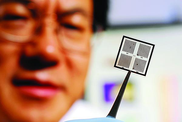
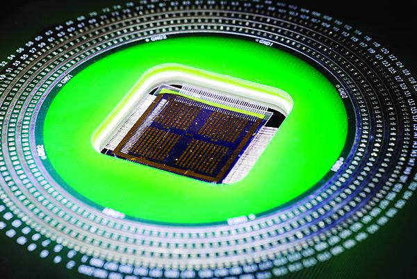
The nanoscale zinc oxide wires are at the heart of PRM and piezotronic processes. Georgia Tech researchers made use of large-scale fabrication techniques for the nanowire arrays, which allowed multiple arrays to be built and tested. Wang believes that the work represents a major advance in nanoscale piezoelectrics. “We made a breakthrough in the field,” he maintains.
The breakthrough claim is based on the novelty of the piezotronic effect and because the researcher’s laboratory made an array of devices with PRM components. Wang notes that in the scientific literature on nanotechnology, most researchers rarely make more than one or two devices. “We made an array of 20 devices. Each one is a sensor or a piezotronic transistor that can work independently and in parallel,” he says. All of the devices consisted of thousands of nanowires.
To achieve this breakthrough, the Georgia Tech researchers developed a top-down fabrication process to make the piezoelectric nanowires. The lab also has the lithography and chemical capabilities to control the growth of the wires precisely, factoring in their orientation, density, dimension and other elements. Because the wires can be produced in numbers to such high control standards, researchers could apply them to a variety of devices.
But perfecting the fabrication process was difficult. It took the team 31 steps to complete fully the integrated PRM production system, Wang says. A single mistake in any preceding step meant that the researchers had to begin the process from the beginning again, he adds.
The zinc oxide nanowires are about 500 nanometers in diameter and 50 microns long. They are produced through a physical vapor deposition process that uses a high-temperature furnace. The raw structures then are treated with oxygen plasma to reduce the number of crystalline defects, which helps control their conductivity. The arrays are them placed on a flexible substrate.
The switching voltage on the devices can be tuned depending on the number of oxygen vacancies in the structure, Wang says. He notes that the more defects quenched with the oxygen plasma, the larger the voltage needed to drive the current flow. Additionally, the piezotronic memory cells operate at low frequencies, which makes them appropriate for the types of biologically generated signals they will record, he adds.
The next step in the technology is to improve the stability of the nanowire devices for practical applications, Wang explains. Another goal is improving the devices’ density and resolution for very-high-resolution applications. Researchers also want to interface PRM technology with other electronic technologies, such as silicon-based microprocessors or biologically related technology. The goal is to create interfaces that can be used directly in practical applications. “We hope to make something that is really high performance and which is really useful,” he says.


Comments